11. Calculate the maximum Thevenin equivalent resistance, if a 10kΩ potentiometer is used?
A. 0.4kΩ
B. 5 kΩ
C. 2.5kΩ
D. 4kΩ
Answer: C
Rmax= Ra/2 || Ra/2 = Ra/4.
Given potentiometer, Ra = 10kΩ
=> Therefore, Rmax = 10kΩ/4 =2.5kΩ.
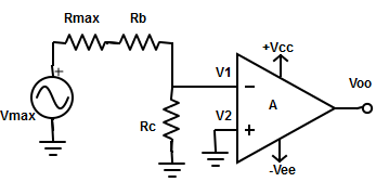
12. Find the input offset voltage for the circuit shown
A. Vio = (Rb*Vmax)/( Rmax+ Rb+ Rc)
B. Vio = Rmax/( Rmax+ Rb+ Rc)
C. Vio = (Rc*Vmax)/( Rmax+ Rb+ Rc)
D. Vio = Vmax/( Rmax+ Rb+ Rc)
Answer: C
Compensating network using maximum Thevenin’s equivalent for resistance and voltage circuit is shown. Since |V1-V2|- Vio, the maximum value of V2 can be equal to Vio.
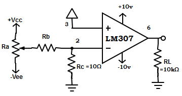
13. Find the value of Ra and Rb from the circuit shown?
A. Ra =4.6kΩ ; Rb= 9kΩ
B. Ra =7.3kΩ ; Rb= 3.4kΩ
C. Ra =2.5kΩ ; Rb= 5.1kΩ
D. Ra =4kΩ ; Rb= 10kΩ
Answer: D
We know that input offset voltage, Vio =(Rc*Vmax)/ Rb
=> Rb = Vmax*(Rc / Rb )
= (10v/10mv)*10Ω (∵ Vio specified on the datasheet is 10mv for LM307 op-amp).
=> Rb =10000 = 10kΩ.
Since Rb > Rmax let us choose Rb = 10*Rmax. (Where Rmax = Ra/4).
∴ Rb = (10*Rb)/4 and Ra = Rb/2.5
= 10kΩ/2.5=4kΩ.
14. Why does an op-amp without feedback is not used in linear circuit application?
A. Due to high current gain
B. Due to high voltage gain
C. Due to high output signal
D. All of the mentioned
Answer: B
In an op-amp without feedback, the voltage gain is extremely high (ideally infinite). Because of the high risk of distortion and clipping of the output signal, an op-amp in open loop configuration is not used in linear circuit applications.
15. When the input voltage is reduced to zero in a closed-loop configuration the circuit acts as?
A. Inverting amplifier
B. Non-inverting amplifier
C. Inverting and non-inverting amplifier
D. None of the mentioned
Answer: C
Since the input signal voltage is reduced to zero, the internal resistance is negligibly small. The output offset voltage is expressed in terms of external resistance and the specified input offset voltage for a given op-amp.
If the non-inverting input terminal is connected to the ground, it acts as inverting op-amp and vice versa.
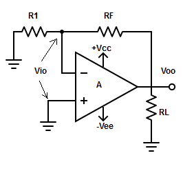
16. How the value of output offset voltage is reduced in closed-loop op-amp?
A. By increasing gain
B. By reducing the gain
C. By decreasing bandwidth
D. By reducing bandwidth
Answer: B
The output offset voltage is a product of gain and specified input offset voltage for a given op-amp. Voo= Aoo*Vio. So, the value of output offset voltage can be reduced by reducing the gain value.
17. What happens if R1>>RF in the circuit
A. Some amount of output offset voltage is present
B. Some amount of input offset voltage is present
C. Some amount of gain voltage is present
D. All of the mentioned
Answer: A
If R1 >>RF, the gain Aoo≅1, which makes Voo ≅ Vio. Thus, all op-amp circuit has some output offset voltage.
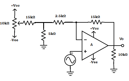
18. Determine the voltage gain for the circuit.
A. 1.1
B. 1.6
C. 1.2
D. 2.2
Answer: D
The voltage gain,
AF={1+[RF/( R1+ Rc)]}
= 1+[15kΩ/(2.5kΩ+10kΩ)] = 2.2.
19. Where does the compensating network connected in an inverting amplifier?
A. Non-inverting input terminal
B. Inverting input terminal
C. Between non-inverting and output terminal
D. Between inverting and output terminal
Answer: A
The offset voltage compensating network is connected to the non-inverting terminal for the inverting amplifier and vice versa.
20. Why closed-loop differential amplifiers are difficult to null?
A. Due to compensating network
B. Due to the feedback loop
C. Due to the input offset voltage
D. None of the mentioned
Answer: A
The closed-loop differential amplifiers are more difficult to null because the use of compensating network can change the common-mode rejection mode.